First, based on MF RC500 developed cost-effective Mifare card reader module
The MF RC500 is mainly used for reading and writing 13.56MHz contactless IC cards. The chip utilizes advanced modulation and demodulation concepts and fully integrates all types of passive contactless communication methods and protocols at 13.56 MHz. The MF RC500 supports all layers of the ISO14443A (13.56MHz electronic label standard). The internal transmitter section can directly drive a close-range antenna (up to 10 cm) without adding active circuitry. The receiver section provides a reliable and efficient demodulation and decoding circuit for ISO14443A compatible transponder signals. The digital part handles ISO14443A frame and error detection. In addition, it supports the fast CRYPTO1 encryption algorithm for validating the MIFARE family of products. The convenient parallel interface allows direct connection to any 8-bit microprocessor, which provides great flexibility in the design of the reader/terminal. Figure 2 shows the schematic of the peripheral circuit of the MFRC500.
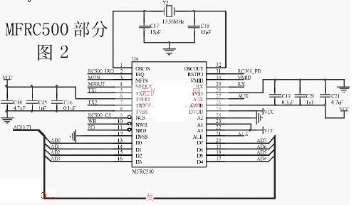
Second, MF RC500 pin function introduction
1, the oscillator
name
Types of
Features
OSCIN
Input
Crystal input
OSCOUT
Output
Crystal output
The 1-pin OSCIN and 2-pin OSCOUT of the MFRC500 are the crystal input and the crystal output, respectively. The 13.56MHz crystal is connected to OSCIN and OSCOUT via a fast on-chip buffer. If the device uses an external clock, it can be input from OSCIN.
2, the antenna
The contactless antenna uses the following 4 pins:
name
Types of
Features
TX1, TX2
Output buffer
Antenna driver
VMID
simulation
Reference voltage
RX
Input simulation
Antenna input signal
To drive the antenna, the MF RC500 provides an energy carrier of 13.56 MHz through TX1 and TX2. The transmitted data is modulated according to the setting of the register to obtain a transmitted signal. The card responds with load modulation of the RF field. The signal picked up by the antenna is sent to the RX pin through the antenna matching circuit. The MF RC500 internal receiver detects and demodulates the signal and processes it according to the settings of the register. The data is then sent to the parallel interface for reading by the microcontroller. The antenna part of the circuit diagram is as shown in (Figure 3). 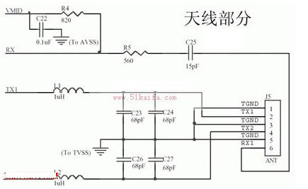
3, the power supply
The device MF RC500 uses separate power supplies for each part to achieve optimum performance in terms of EMC characteristics and signal decoupling. The MF RC500 has excellent RF performance and the analog and digital sections can be adapted to different operating voltages.
name
Types of
Features
TVDD
power supply
Transmitter supply voltage
VSS
power supply
Transmitter power ground
AVDD
power supply
Analog part supply voltage
AGND
power supply
Analog part power ground
DVDD
power supply
Digital part supply voltage
DVSS
power supply
Digital part power ground
4. Auxiliary Pin MF RC500's 27th pin AUX is the auxiliary pin. The internal signal can be selected to drive the pin. It can be used for design and testing.
5. Reset pin RSTPD is the reset pin. This pin disables the internal current source and clock and disconnects the MF RC500 from the microcontroller bus interface. If the RST is released, the MF RC500 performs the power-up sequence.
6. Serial signal switch The serial signal switch is used to bridge the chip digital circuit and the analog circuit. The input/output of the two-part circuit and the input/output required for the external application can be flexibly combined. This combination can be controlled by means of the MFIN and MFOUT pins and the MF RC500 internal related registers.
name
Types of
Features
MFIN
Input with Schmitt trigger
MIFARE interface input
MFOUT
Output
MIFARE interface output
7, parallel interface
The 16 pins listed below are used to control the parallel interface:
name
Types of
Features
D0 ... D7
I/O with Schmitt trigger
Bidirectional data bus
A0 ... A2
I/O with Schmitt trigger
Address line
NWR/RNW
I/O with Schmitt trigger
Write disable / read only
NRD/NDS
I/O with Schmitt trigger
Read prohibit/data strobe prohibition
NCS
I/O with Schmitt trigger
Chip selection prohibited
ALE
I/O with Schmitt trigger
Address latch enable
IRQ
Output
Interrupt request
Third, the interface circuit of MF RC500 and 89C51 (Figure 4):
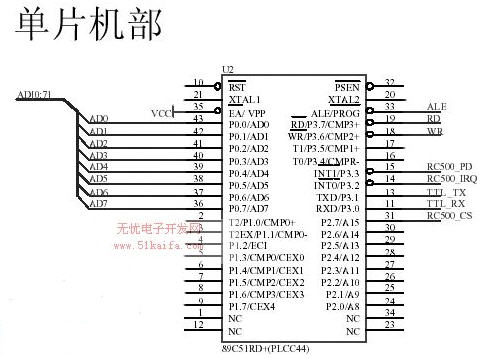
The MF RC500 supports different microcontroller interfaces. An intelligent automatic detection logic automatically adapts to the parallel interface of the system bus. The chip is selected using the signal NCS. To connect to the microcontroller using a separate address and data bus, the ALE pin must be connected to the DVDD. If a multiplexed address and data bus is used to interface with the microcontroller, the ALE pin must be connected to the ALE signal of the microcontroller. To connect to the microcontroller using RNW and NDS (instead of NWR and NRD), the RNW of the microcontroller must be connected to pin NWR and the NDS must be connected to the NRD. As can be seen from Figure 4, the system uses the interrupt (INT1) mode of operation, that is, the MCU uses the MF RC500 to provide interrupt information to control it. In addition, according to the needs of the system, the MF RC500 can be operated by query. The Mifare card operation process consists of the following parts:
1, reset request
Sector number
Block number
content
Block address
Sector 0
0 block
Vendor code
0
1 block
Data (16 bytes)
1
2 pieces
Data (16 bytes)
2
3 blocks
password area
3
Sector 1
0 block
Data (16 bytes)
4
1 block
Data (16 bytes)
5
2 pieces
Data (16 bytes)
6
3 blocks
password area
7
.
:
:
:
Sector 15
0 block
Data (16 bytes)
60
1 block
Data (16 bytes)
61
2 pieces
Data (16 bytes)
62
3 blocks
password area
63
When a Mifare card is within the working range of the antenna of the reader at the card, the programmer controls the reader to issue a reset command to the card. After the card is received, the manufacturer code in the 0 block 0 block (as a different card type) is sent to the Mifare card (using the M1 card as an example). The internal storage structure is as follows [5]. Establish the first communication link between the card and the reader.
2. Anti-collision operation If there are multiple Mifare cards in the working range of the card reader's antenna, the module will first communicate with each card to obtain the serial number of each card. Since each Mifare card has its unique serial number, it will never be the same, so it is guaranteed to operate on only one card at a time according to the serial number of the card.
3. After the card selection operation has completed the above two steps, the read/write module must perform a selection operation on the card. The data is exchanged with the selected card. When a card is selected, the card transfers its data capacity to the reader/writer.
4. Authentication operation After the above three steps, when confirming that a card has been selected, the program control module must authenticate the password already set on the card before the card is read and written, and the encryption algorithm in the Mifare product. The implementation is called CRYPT01, which is a stream cipher with a key length of 48 bits. To access data for a Mifare class card, you must first complete the certification. If it matches, further read and write operations are allowed.
5, read and write operations The final operation of the card is read, write, value-added, depreciation, storage and transfer operations.
Salon Nails Kit,Golden French Gray False Nails,Short Square Artificial Nails,Super Thin Short False Nails
Zhong Shan Senboma Artware Co.,Ltd , https://www.senbomanails.com